0
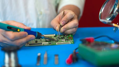
Printed circuit boards (PCBs) are the boards that are used as the base in most electronics – both as a physical support piece and as the wiring area for the surface-mounted and socketed components. PCBs are most commonly made out of fiberglass, composite epoxy, or another composite material.
Most PCBs for simple electronics are simple and composed of only a single layer. More sophisticated hardware such as computer graphics cards or motherboards can have multiple layers, sometimes up to twelve.
There are several overall types of PCB boards each with their own particular manufacturing specifications, material types, and usages: Single-layer PCBs, Double-layer PCBs, Multi-layer PCBs, Rigid PCBs, Flexible PCBs, Rigid-Flex PCBs, High-frequency PCBs, Aluminum-backed PCBs.
PCB Soldering Geeks
Wiki User
∙ 14y agoA PCB is a printed circuit board.
Add your answer:
What is the effect of air bubble in PCB laminated process?
There will be a poor bonding between copper and prepreg in the bubbled area, this leads yo delamination or bulging of PCB.
How much does a PCB cost?
First, I am assuming that by PCB you mean Printed Circuit Board. Next, this depends upon many, many factors, none of which are "givens" here. There is quantity. You can order anything from a prototype run of say 6 to a major production run of say 6 million. The more you order, the more highly tooled production will be, the lower the unit cost. The second factor is size of the PCB. If all else is the same, cost will be roughly proportional to size (meaning to area), so all else equal, a 12 inch by 12 inch PCB will be 4 times as costly as a 6 inch by 6 inch. Next is material. Very inexpensive materials such as Phenolic cotton paper, can be used in simple toys (although safety will be an issue). Top-of-the-line electronics is more likely to use materials like Teflon, glass, epoxy, and polyester. Structure is a major factor. The simplest, and cheapest PCB is an insulator like Phenolic-cotton-paper with a copper layer on one side. At the other end, we have many layer PCB's (for-instance 24 layer) with thru-holes interconnecting the layers. There can be contact fingers which are part of a PCB. One set for a plug-in PCB, many sets for a system board which goes to many other devices. Finally, there are finishing elements such as solder masks and silk screens. All that said, a small very simple high volume PCB might be as low as $0.10 USD. An elegant, low volume multilayer PCB with full bells and whistles might cost $1000.00 USD.
Advantages and disadvantages of using a veroboard?
No drilling holes Quick to assemble Quick to change components arround you need all the components to make circuit more expensive than PCB and Breadboard
How do you make calls from galaxy tab 10.1?
You can´t make phone calls with 10.1 unless you use skype or other app for this.
What is false answer supervision?
when you are calling , in the distenation show duration befor answer call and use charge and this is problem on the network (VOIP)
When was PCB Piezotronics created?
PCB Piezotronics was created in 1967.
Which course better for pcb design?
pcb design at ramanthapur ATI
What is the nickname of Pakistan cricket team?
PCB PCB is tha nick name of Pakistan cricket team and Also Green Shirts.
What does a pcb manufacturer do?
In this specific job what you would be doing as a pcb manufacturer, you would be manufacturing printed circuit boards. This is what the job description of a pcb is.
When was DesignSpark PCB created?
DesignSpark PCB was created on 2010-07-05.
What does pcb mean in design and teconolady?
It means Printed Circuit Board (PCB)
What is the full form of PCB?
PCB stands for "Polychlorinated biphenyl" in chemistry and environmental protection. PCB stands for "printed circuit board" in electrical engineering.
Is typical thickness of pcb 2mm?
The standard pcb thickness is 1.57mm, 0.063", or 63 mil.
What is the average cost of pcb design software?
"The average cost of PCB design software is $200.
What is a PCB layout used for?
Short for printed circuit board, a PCB is a component in most electronic components. Typically, PCB layouts are used to help support the components mechanically.
Why etching is done on PCB?
pcb is a copper sheet. once we prepare the layout, we need the tracks which gets covered by copper.Therefore, to remove excess copper from the pcb etching is done.
What is the PCB and its location?
PCB technologies is an information technology company in Johannesburg, South Africa. A PCB populated with electronic components is called a printed circuit assembly (PCA), printed circuit board assembly or PCB assembly (PCBA). In informal usage, the term "printed circuit board" most commonly means "printed circuit assembly" (with components).